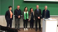
Céline Noel : PhD defence
The PhD was defended on the 8th of april 2019, in presence of the jury :
Dr. Yan Busby (UNamur)
Dr. Francesca Cecchet (UNamur)
Prof. Arnaud Delcorte (UCLouvain)
Prof. Anouk Galtayries (Chimie Paris Tech)
Prof. Laurent Houssiau (Supervisor, UNamur)
Abstract
In diverse areas such as medicine, energy, aerospace or electronics, the technology around us is constantly growing in sophistication. To improve device performances, advanced materials are combined into thin films multilayers or to form complex 3D architectures.
At the same time, the search for miniaturization pushes the device features to dimensions in the nanometer range, which confers a preponderant role to interfaces in the macroscopic behavior of devices. The understanding of complex phenomena taking place at thin films interfaces is mandatory to identify degradation mechanisms and also to rationally prevent or limit these effects. Therefore, methods for in-depth characterization need to be developed to implement strategies and to guide both the design and the processing conditions of thin film stacks; this would finally allow increasing both the device performance and lifetime.
In this context, time-of-flight secondary ion mass spectrometry (ToF-SIMS) has shown its ability to provide in-depth molecular information, combining an extremely high detection limit and surface sensitivity, high mass and depth resolutions, and convenient lateral resolution to image 3D features.
In this thesis work, ToF-SIMS surface and depth profile analysis is applied to investigate model and applied thin film architectures using different analysis and erosion ion beams conditions. In particular, the fundamental interaction mechanisms between ion beams and materials surfaces are highlighted by varying the nature, energy and size of the ion beam projectile. For hybrid (organic/inorganic) thin films, the sputtering and analysis beams conditions have been optimized to limit the materials modifications induced by the ion beam exposure while maintaining intense and characteristic (high mass fragments) molecular signals and reasonable sputtering yields (i.e. analysis time).
On particularly challenging hybrid device architectures for OLEDs and solar cells applications, the results unambiguously show that low energy cesium ion beam (Cs+ at ~ 500 eV) and argon clusters ion beams (Arn+) with reduced size (n~500 atoms) at a relatively high energy (~20 keV) are the most suitable conditions to perform depth profile analysis.


